 | –≠–ª–µ–∫—Ç—Ä–æ–Ω–Ω—ã–π –∫–æ–º–ø–æ–Ω–µ–Ω—Ç: SP514 | –°–∫–∞—á–∞—Ç—å:  PDF PDF  ZIP ZIP |
1
Rev. 3/05/04
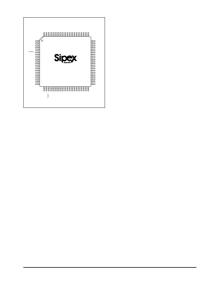
SP514 Multi≠Mode Serial Transceiver
© Copyright 2004 Sipex Corporation
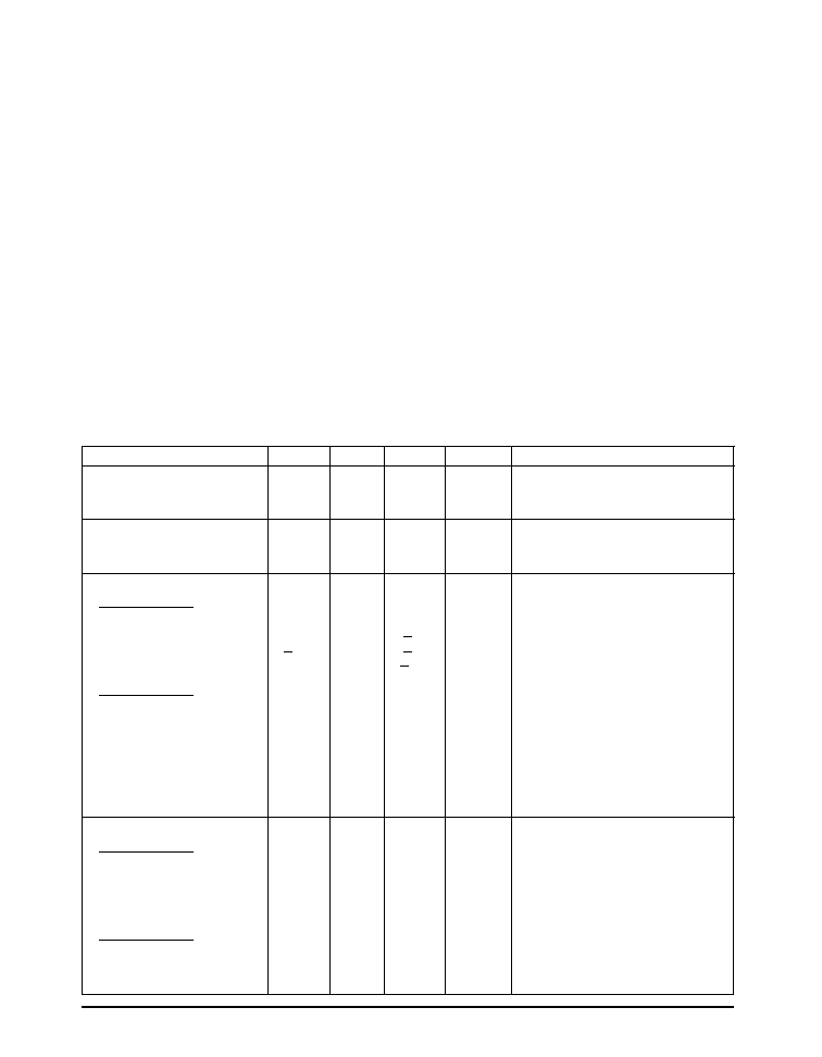
The SP514 is a single chip devices that supports eight (8) physical serial interface standards
for Wide Area Network connectivity. The product is fabricated using a low power BiCMOS
process technology, and incorporates a Sipex patented (5,306,954) charge pump allowing
+5V only operation. The SP514 is 100% compatible with the SP504 multi-protocol serial
transceiver IC. All applications using the SP504 can also use the SP514. The SP514 has
slightly improved AC performance for its V.35 and V.11 drivers and receivers.
DESCRIPTION
+5V Only
Seven (7) Drivers and Seven (7) Receivers
Driver and Receiver Tri-State Control
Reduced V.35 Termination Network
Pin Compatible with the SP504
Improved Propagation Delays
Software Selectable Interface Modes:
-RS-232E (V.28)
-RS-422A (V.11, X.21)
-RS-449 (V.11 & V.10)
-RS-485
-V.35
-EIA-530 (V.11 & V.10)
-EIA-530A (V.11 & V.10)
-V.36
SP514
WAN Multi-Mode Serial Transceiver
EIA-530
WAN
V.35
Æ
2
Rev. 3/05/04
SP514 Multi≠Mode Serial Transceiver
© Copyright 2004 Sipex Corporation
SPECIFICATIONS
T
A
= +25
∞
C and V
CC
= +4.75V to +5.25V unless otherwise noted.
MIN.
TYP.
MAX.
UNITS
CONDITIONS
LOGIC INPUTS
V
IL
0.8
Volts
V
IH
2.0
Volts
LOGIC OUTPUTS
V
OL
0.4
Volts
I
OUT
= ≠3.2mA
V
OH
2.4
Volts
I
OUT
= 1.0mA
V.28 DRIVER
DC Parameters
Outputs
Open Circuit Voltage
+15
Volts
per Figure 1
Loaded Voltage
+5.0
+15
Volts
per Figure 2
Short-Circuit Current
+100
mA
per Figure 4
Power-Off Impedance
300
per Figure 5
AC Parameters
V
CC
= +5V & T
A
= +25
∞
C for AC parameters
Outputs
Transition Time
1.5
µ
s
per Figure 6; +3V to -3V
Instantaneous Slew Rate
30
V/
µ
s
per Figure 3
Propagation Delay
t
PHL
0.5
1
5
µ
s
t
PLH
0.5
1
5
µ
s
Max.Transmission Rate
120
230
kbps
V.28 RECEIVER
DC Parameters
Inputs
Input Impedance
3
7
k
per Figure 7
Open-Circuit Bias
+2.0
Volts
per Figure 8
HIGH Threshold
1.7
3.0
Volts
LOW Threshold
0.8
1.2
Volts
AC Parameters
V
CC
= +5V & T
A
= +25
∞
C for AC parameters
Propagation Delay
t
PHL
50
100
500
ns
t
PLH
50
100
500
ns
ABSOLUTE MAXIMUM RATINGS
These are stress ratings only and functional operation
of the device at these ratings or any other above those
indicated in the operation sections of the specifications
below is not implied. Exposure to absolute maximum
rating conditions for extended periods of time may
affect reliability.
V
CC
............................................................................+7V
Input Voltages:
Logic...............................-0.3V to (V
CC
+0.5V)
Drivers............................-0.3V to (V
CC
+0.5V)
Receivers........................................
±
15.5V
Output Voltages:
Logic................................-0.3V to (V
CC
+0.5V)
Drivers................................................
±
15V
Receivers........................-0.3V to (V
CC
+0.5V)
Storage Temperature..........................-65∞C to +150∞C
Power Dissipation.........................................2000mW
Package Derating:
¯
JA
....................................................46
∞
C/W
¯
JC
...................................................16
∞
C/W
STORAGE CONSIDERATIONS
Due to the relatively large package size of the 80-pin
quad flat-pack, storage in a low humidity environment
is preferred. Large high density plastic packages are
moisture sensitive and should be stored in Dry Vapor
Barrier Bags. Prior to usage, the parts should remain
bagged and stored below 40
∞
C and 60%RH. If the
parts are removed from the bag, they should be used
within 48 hours or stored in an environment at or below
20%RH. If the above conditions cannot be followed,
the parts should be baked for four hours at 125
∞
C in
order remove moisture prior to soldering. Sipex ships
the 80-pin QFP in Dry Vapor Barrier Bags with a
humidity indicator card and desiccant pack.The
humidity indicator should be below 30%RH.

3
Rev. 3/05/04
SP514 Multi≠Mode Serial Transceiver
© Copyright 2004 Sipex Corporation
SPECIFICATIONS
T
A
= +25
∞
C and V
CC
= +4.75V to +5.25V unless otherwise noted.
MIN.
TYP.
MAX.
UNITS
CONDITIONS
V.28 RECEIVER (continued)
AC Parameters (cont.)
Max.Transmission Rate
120
230
kbps
V.10 DRIVER
DC Parameters
Outputs
Open Circuit Voltage
+4.0
+6.0
Volts
per Figure 9
Test-Terminated Voltage
0.9V
OC
Volts
per Figure 10
Short-Circuit Current
+150
mA
per Figure 11
Power-Off Current
+100
µ
A
per Figure 12
AC Parameters
V
CC
= +5V & T
A
= +25
∞
C for AC parameters
Outputs
Transition Time
100
ns
per Figure 13; 10% to 90%
Propagation Delay
t
PHL
50
200
1000
ns
t
PLH
50
200
1000
ns
Max.Transmission Rate
120
kbps
V.10 RECEIVER
DC Parameters
Inputs
Input Current
≠3.25
+3.25
mA
per Figures 14 and 15
Input Impedance
4
k
Sensitivity
+0.3
Volts
AC Parameters
V
CC
= +5V & T
A
= +25
∞
C for AC parameters
Propagation Delay
t
PHL
50
120
250
ns
t
PLH
50
120
250
ns
Max.Transmission Rate
120
kbps
V.11 DRIVER
DC Parameters
Outputs
Open Circuit Voltage
+6.0
Volts
per Figure 16
Test Terminated Voltage
+2.0
Volts
per Figure 17
0.5V
OC
0.67V
OC
Volts
Balance
+0.4
Volts
per Figure 17
Offset
+3.0
Volts
per Figure 17
Short-Circuit Current
+150
mA
per Figure 18
Power-Off Current
+100
µ
A
per Figure 19
AC Parameters
V
CC
= +5V & T
A
= +25
∞
C for AC parameters
Outputs
Transition Time
20
40
ns
per Figures 21 and 36; 10% to 90%
Propagation Delay
Using R
L
= 100
and C
L
= 50pF;
t
PHL
50
75
95
ns
per Figures 32 and 36
t
PLH
50
75
95
ns
per Figures 32 and 36
Differential Skew
20
40
ns
per Figures 32 and 36
Max.Transmission Rate
10
Mbps
V.11 RECEIVER
DC Parameters
Inputs
Common Mode Range
≠7
+7
Volts
Sensitivity
+0.3
Volts
4
Rev. 3/05/04
SP514 Multi≠Mode Serial Transceiver
© Copyright 2004 Sipex Corporation
SPECIFICATIONS
T
A
= +25
∞
C and V
CC
= +4.75V to +5.25V unless otherwise noted.
MIN.
TYP.
MAX.
UNITS
CONDITIONS
V.11 RECEIVER (continued)
DC Parameters (cont.)
Input Current
≠3.25
+3.25
mA
per Figure 20 and 22
Current w/ 100
Termination
+60.75
mA
per Figure 23 and 24
Input Impedance
4
k
AC Parameters
V
CC
= +5V & T
A
= +25
∞
C for AC parameters
Propagation Delay
Using R
L
= 100
and C
L
= 50pF;
t
PHL
60
100
125
ns
per Figures 32 and 38
t
PLH
60
100
125
ns
per Figures 32 and 38
Differential Skew
20
ns
per Figure 32
Max. Transmission Rate
10
Mbps
V.35 DRIVER
DC Parameters
Outputs
Test Terminated Voltage
+0.44
+0.66
Volts
per Figure 25
Offset
+0.6
Volts
per Figure 26
Source Impedance
50
150
per Figure 27
Short-Circuit Impedance
135
165
per Figure 28
AC Parameters
V
CC
= +5V & T
A
= +25
∞
C for AC parameters
Outputs
Transition Time
30
60
ns
per Figure 29; 10% to 90%
Propagation Delay
t
PHL
50
75
95
ns
per Figures 33 and 36
t
PLH
50
75
95
ns
per Figures 33 and 36
Differential Skew
20
40
ns
per Figures 33 and 36
Max.Transmission Rate
10
Mbps
V.35 RECEIVER
DC Parameters
Inputs
Sensitivity
80
mV
Source Impedance
90
110
per Figure 30
Short-Circuit Impedance
135
165
per Figure 31
AC Parameters
V
CC
= +5V & T
A
= +25
∞
C for AC parameters
Propagation Delay
t
PHL
60
115
125
ns
per Figures 33 and 38
t
PLH
60
115
125
ns
per Figures 33 and 38
Differential Skew
20
ns
per Figure 33
Max. Transmission Rate
10
Mbps
POWER REQUIREMENTS
V
CC
4.75
5.00
5.25
Volts
I
CC
(No Mode Selected)
30
mA
All I
CC
values are with V
CC
= +5V
(V.28/RS-232)
130
mA
f
IN
= 120kbps; Drivers active & loaded.
(V.11/RS-422)
280
mA
f
IN
= 2.1Mbps; Drivers active & loaded.
(EIA-530 & RS-449)
250
mA
f
IN
= 2.1Mbps; Drivers active & loaded.
(V.35)
180
mA
V.35 @ f
IN
= 2.1Mbps, V.28 @ 20kbps;
Drivers active & loaded.
ENVIRONMENTAL AND MECHANICAL
Operating Temperature Range
0
+70
∞
C
Storage Temperature Range
≠65
+150
∞
C

5
Rev. 3/05/04
SP514 Multi≠Mode Serial Transceiver
© Copyright 2004 Sipex Corporation
OTHER AC CHARACTERISTICS
T
A
= +25
∞
C and V
CC
= +5.0V unless otherwise noted.
PARAMETER
MIN.
TYP.
MAX.
UNITS
CONDITIONS
DRIVER DELAY TIME BETWEEN ACTIVE MODE AND TRI-STATE MODE
RS-232/V.28 MODE
t
PZL
; Tri-state to Output LOW
0.70
5.0
µ
s
C
L
= 100pF, Fig. 34 ; S
1
closed
t
PZH
; Tri-state to Output HIGH
0.40
2.0
µ
s
C
L
= 100pF, Fig. 34 ; S
2
closed
t
PLZ
; Output LOW to Tri-state
0.20
2.0
µ
s
C
L
= 100pF, Fig. 34 ; S
1
closed
t
PHZ
; Output HIGH to Tri-state
0.40
2.0
µ
s
C
L
= 100pF, Fig. 34 ; S
2
closed
RS-423/V.10 MODE
t
PZL
; Tri-state to Output LOW
0.15
2.0
µ
s
C
L
= 100pF, Fig. 34 ; S
1
closed
t
PZH
; Tri-state to Output HIGH
0.20
2.0
µ
s
C
L
= 100pF, Fig. 34 ; S
2
closed
t
PLZ
; Output LOW to Tri-state
0.20
2.0
µ
s
C
L
= 100pF, Fig. 34 ; S
1
closed
t
PHZ
; Output HIGH to Tri-state
0.15
2.0
µ
s
C
L
= 100pF, Fig. 34 ; S
2
closed
RS-422/V.11 MODE
t
PZL
; Tri-state to Output LOW
2.80
10.0
µ
s
C
L
= 100pF, Fig. 34 & 37; S
1
closed
t
PZH
; Tri-state to Output HIGH
0.10
2.0
µ
s
C
L
= 100pF, Fig. 34 & 37; S
2
closed
t
PLZ
; Output LOW to Tri-state
0.10
2.0
µ
s
C
L
= 15pF, Fig. 34 & 37; S
1
closed
t
PHZ
; Output HIGH to Tri-state
0.10
2.0
µ
s
C
L
= 15pF, Fig. 34 & 37; S
2
closed
V.35 MODE
t
PZL
; Tri-state to Output LOW
2.60
10.0
µ
s
C
L
= 100pF, Fig. 34 & 37; S
1
closed
t
PZH
; Tri-state to Output HIGH
0.10
2.0
µ
s
C
L
= 100pF, Fig. 34 & 37; S
2
closed
t
PLZ
; Output LOW to Tri-state
0.10
2.0
µ
s
C
L
= 15pF, Fig. 34 & 37; S
1
closed
t
PHZ
; Output HIGH to Tri-state
0.15
2.0
µ
s
C
L
= 15pF, Fig. 34 & 37; S
2
closed
RECEIVER DELAY TIME BETWEEN ACTIVE MODE AND TRI-STATE MODE
RS-232 MODE
t
PZL
; Tri-state to Output LOW
0.12
2.0
µ
s
C
L
= 100pF, Fig. 35 ; S
1
closed
t
PZH
; Tri-state to Output HIGH
0.10
2.0
µ
s
C
L
= 100pF, Fig. 35 ; S
2
closed
t
PLZ
; Output LOW to Tri-state
0.10
2.0
µ
s
C
L
= 100pF, Fig. 35 ; S
1
closed
t
PHZ
; Output HIGH to Tri-state
0.10
2.0
µ
s
C
L
= 100pF, Fig. 35 ; S
2
closed
RS-423 MODE
t
PZL
; Tri-state to Output LOW
0.10
2.0
µ
s
C
L
= 100pF, Fig. 35 ; S
1
closed
t
PZH
; Tri-state to Output HIGH
0.10
2.0
µ
s
C
L
= 100pF, Fig. 35 ; S
2
closed
t
PLZ
; Output LOW to Tri-state
0.10
2.0
µ
s
C
L
= 100pF, Fig. 35 ; S
1
closed
t
PHZ
; Output HIGH to Tri-state
0.10
2.0
µ
s
C
L
= 100pF, Fig. 35 ; S
2
closed
RS-422/RS-485 MODES
t
PZL
; Tri-state to Output LOW
0.10
2.0
µ
s
C
L
= 100pF, Fig. 35 & 39; S
1
closed
t
PZH
; Tri-state to Output HIGH
0.10
2.0
µ
s
C
L
= 100pF, Fig. 35 & 39; S
2
closed
t
PLZ
; Output LOW to Tri-state
0.10
2.0
µ
s
C
L
= 15pF, Fig. 35 & 39; S
1
closed
t
PHZ
; Output HIGH to Tri-state
0.10
2.0
µ
s
C
L
= 15pF, Fig. 35 & 39; S
2
closed
V.35 MODE
t
PZL
; Tri-state to Output LOW
0.10
2.0
µ
s
C
L
= 100pF, Fig. 35 & 39; S
1
closed
t
PZH
; Tri-state to Output HIGH
0.10
2.0
µ
s
C
L
= 100pF, Fig. 35 & 39; S
2
closed
t
PLZ
; Output LOW to Tri-state
0.10
2.0
µ
s
C
L
= 15pF, Fig. 35 & 39; S
1
closed
t
PHZ
; Output HIGH to Tri-state
0.10
2.0
µ
s
C
L
= 15pF, Fig. 35 & 39; S
2
closed

6
Rev. 3/05/04
SP514 Multi≠Mode Serial Transceiver
© Copyright 2004 Sipex Corporation
OTHER AC CHARACTERISTICS
(Continued)
T
A
= +25
∞
C and V
CC
= +5.0V unless otherwise noted.
TRANSCEIVER TO TRANSCEIVER SKEW
(PER FIGURES 32, 33, 36, 38)
RS-232 Driver
100
ns
[ (t
phl
)
Tx1
≠ (t
phl
)
Tx6,7
]
100
ns
[ (t
plh
)
Tx1
≠ (t
plh
)
Tx6,7
]
RS-232 Receiver
20
ns
[ (t
phl
)
Rx1
≠ (t
phl
)
Rx2,7
]
20
ns
[ (t
phl
)
Rx1
≠ (t
phl
)
Rx2,7
]
RS-422 Driver
2
ns
[ (t
phl
)
Tx1
≠ (t
phl
)
Tx6,7
]
2
ns
[ (t
plh
)
Tx1
≠ (t
plh
)
Tx6,7
]
RS-422 Receiver
3
ns
[ (t
phl
)
Rx1
≠ (t
phl
)
Rx2,7
]
3
ns
[ (t
phl
)
Rx1
≠ (t
phl
)
Rx2,7
]
RS-423 Driver
5
ns
[ (t
phl
)
Tx2
≠ (t
phl
)
Tx3,4,5
]
5
ns
[ (t
plh
)
Tx2
≠ (t
plh
)
Tx3,4,5
]
RS-423 Receiver
5
ns
[ (t
phl
)
Rx2
≠ (t
phl
)
Rx3,4,5
]
5
ns
[ (t
phl
)
Rx2
≠ (t
phl
)
Rx3,4,5
]
V.35 Driver
4
ns
[ (t
phl
)
Tx1
≠ (t
phl
)
Tx6,7
]
4
ns
[ (t
plh
)
Tx1
≠ (t
plh
)
Tx6,7
]
V.35 Receiver
6
ns
[ (t
phl
)
Rx1
≠ (t
phl
)
Rx2,7
]
6
ns
[ (t
phl
)
Rx1
≠ (t
phl
)
Rx2,7
]
7
Rev. 3/05/04
SP514 Multi≠Mode Serial Transceiver
© Copyright 2004 Sipex Corporation
A
V
OC
C
A
V
T
C
3k
A
V
T
C
7k
Oscilloscope
Scope used for slew rate
measurement.
A
I
sc
C
A
C
V
CC
= 0V
±
2V
I
x
A
C
3k
2500pF
Oscilloscope
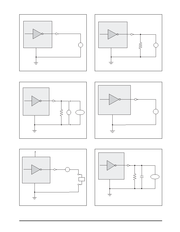
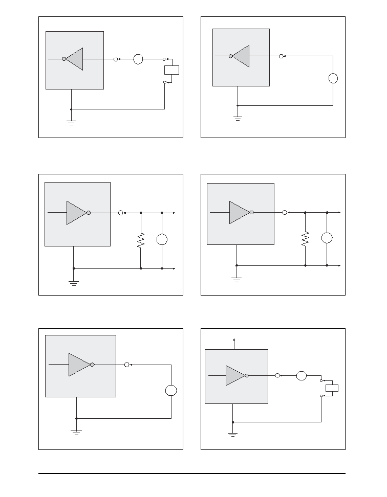
Figure 1. V.28 Driver Output Open Circuit Voltage
Figure 2. V.28 Driver Output Loaded Voltage
Figure 3. V.28 Driver Output Slew Rate
Figure 4. V.28 Driver Output Short-Circuit Current
Figure 6. Driver Output Rise/Fall Times
Figure 5. V.28 Driver Output Power-Off Impedance
TEST CIRCUITS...
8
Rev. 3/05/04
SP514 Multi≠Mode Serial Transceiver
© Copyright 2004 Sipex Corporation
Figure 7. V.28 Receiver Input Impedance
A
C
I
ia
±
15V
A
C
V
oc
Figure 8. V.28 Receiver Input Open Circuit Bias
A
V
OC
3.9k
C
A
V
t
450
C
A
C
±
0.25V
V
CC
= 0V
I
x
A
I
sc
C
Figure 9. V.10 Driver Output Open-Circuit Voltage
Figure 10. V.10 Driver Output Test Terminated Voltage
Figure 12. V.10 Driver Output Power-Off Current
Figure 11. V.10 Driver Output Short-Circuit Current

9
Rev. 3/05/04
SP514 Multi≠Mode Serial Transceiver
© Copyright 2004 Sipex Corporation
Figure 13. V.10 Driver Output Transition Time
Figure 14. V.10 Receiver Input Current
A
450
C
Oscilloscope
A
C
I
ia
±
10V
+3.25mA
≠3.25mA
+10V
+3V
≠3V
≠10V
Maximum Input Current
versus Voltage
V.10 RECEIVER
Figure 15. V.10 Receiver Input IV Graph
Figure 16. V.11 Driver Output Open-Circuit Voltage
A
B
V
OC
3.9k
V
OCA
V
OCB
C
A
B
V
T
50
V
OS
C
50
A
B
C
I
sa
I
sb
Figure 17. V.11 Driver Output Test Terminated Voltage
Figure 18. V.11 Driver Output Short-Circuit Current

10
Rev. 3/05/04
SP514 Multi≠Mode Serial Transceiver
© Copyright 2004 Sipex Corporation
A
B
C
I
xa
±
0.25V
A
B
C
I
xb
±
0.25V
V
CC
= 0V
V
CC
= 0V
A
B
C
I
ia
±
10V
C
I
ib
±
10V
A
B
+3.25mA
≠3.25mA
+10V
+3V
≠3V
≠10V
Maximum Input Current
versus Voltage
V.11 RECEIVER
Figure 19. V.11 Driver Output Power-Off Current
Figure 20. V.11 Receiver Input Current
Figure 21. V.11 Driver Output Rise/Fall Time
Figure 22. V.11 Receiver Input IV Graph
A
B
50
C
50
50
V
E
Oscilloscope
11
Rev. 3/05/04
SP514 Multi≠Mode Serial Transceiver
© Copyright 2004 Sipex Corporation
A
B
C
I
ia
±
6V
C
I
ib
±
6V
A
B
100
to
150
100
to
150
i [mA] = V [V] / 0.1
+6V
+3V
≠3V
≠6V
Maximum Input Current
versus Voltage
V.11 RECEIVER
w/ Optional Cable Termination
(100
to 150
)
i [mA] = V [V] / 0.1
i [mA] = (V [V] ≠ 3) / 4.0
i [mA] = (V [V] ≠ 3) / 4.0
Figure 23. V.11 Receiver Input Current w/ Termination
Figure 24. V.11 Receiver Input Graph w/ Termination
Figure 25. V.35 Driver Output Test Terminated Voltage
Figure 26. V.35 Driver Output Offset Voltage
Figure 27. V.35 Driver Output Source Impedance
A
B
50
C
50
V
T
V
OS
A
B
V
2
50
C
24kHz, 550mV
p-p
Sine Wave
V
1
A
B
50
C
50
V
T
V
OS

12
Rev. 3/05/04
SP514 Multi≠Mode Serial Transceiver
© Copyright 2004 Sipex Corporation
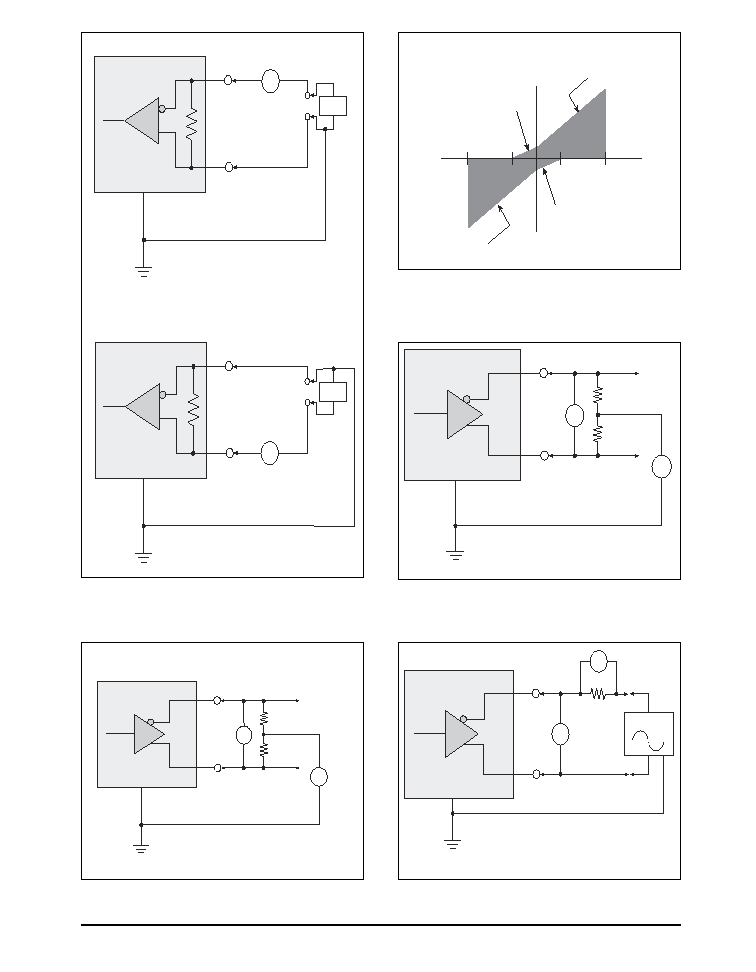
Figure 32. Driver/Receiver Timing Test Circuit
Figure 33. Timing Test Ckt. (V.35 mode only for SP514)
15pF
RO
A
B
A
B
DI
C
L1
15pF
RO
A
B
A
B
DI
C
L2
R
L
Figure 30. V.35 Receiver Input Source Impedance
Figure 29. V.35 Driver Output Rise/Fall Time
Figure 31. V.35 Receiver Input Short-Circuit Impedance
Figure 28. V.35 Driver Output Short-Circuit Impedance
A
B
C
I
SC
±
2V
A
B
C
50
Oscilloscope
50
50
A
B
V
2
50
C
24kHz, 550mV
p-p
Sine Wave
V
1
A
B
C
I
sc
±
2V
13
Rev. 3/05/04
SP514 Multi≠Mode Serial Transceiver
© Copyright 2004 Sipex Corporation
Figure 34. Driver Timing Test Load Circuit
Figure 35. Receiver Timing Test Load Circuit
500
C
L
Output
Under
Test
S
1
S
2
V
CC
1K
1K
C
RL
Receiver
Output
S
1
S
2
Test Point
V
CC
Figure 36. Driver Propagation Delays
+3V
0V
DRIVER INPUT
B
A
DRIVER
OUTPUT
V
O
+
DIFFERENTIAL
OUTPUT
V
A
≠ V
B
0V
V
O
≠
t
SKEW
t
SKEW
1.5V
1.5V
t
PLH
t
R
t
F
f
5MHz; t
R
10ns; t
F
10ns
V
O
1/2V
O
1/2V
O
t
PHL
Figure 37. Driver Enable and Disable Times
+3V
0V
DEC
X
5V
V
OL
A, B
0V
1.5V
1.5V
t
ZL
t
ZH
f = 1MHz; t
R
10ns; t
F
10ns
V
OH
A, B
2.3V
2.3V
t
LZ
t
HZ
0.5V
0.5V
Output normally LOW
Output normally HIGH
TX
ENABLE
Note: Figure 36 shown above is corrected from Figure 5 in SP504 Datasheet. Figure 5 in the SP504 Datasheet is incorrect where A and B are
reversed and the V
A
≠V
B
output should be inverted.
14
Rev. 3/05/04
SP514 Multi≠Mode Serial Transceiver
© Copyright 2004 Sipex Corporation
Figure 39. Receiver Enable and Disable Times
+3V
0V
RDEC
X
5V
0V
1.5V
1.5V
t
ZL
t
ZH
f = 1MHz; t
R
< 10ns; t
F
< 10ns
RECEIVER OUT
1.5V
1.5V
t
LZ
t
HZ
0.5V
0.5V
Output normally LOW
Output normally HIGH
V
IL
V
IH
RECEIVER OUT
Figure 38. Receiver Propagation Delays
V
OH
V
OL
RECEIVER OUT
1.5V
1.5V
t
PHL
f = 1MHz; t
R
10ns; t
F
10ns
OUTPUT
V
OD2
+
V
OD2
≠
A ≠ B
0V
0V
t
PLH
INPUT
Note: Figure 38 shown above is corrected from Figure 7 in the original SP504 Datasheet. Figure 7 in the original SP504 Datasheet is incorrect where
the RECEIVER OUTPUT should be inverted.
15
Rev. 3/05/04
SP514 Multi≠Mode Serial Transceiver
© Copyright 2004 Sipex Corporation
PINOUT...
PIN ASSIGNMENTS...
CLOCK AND DATA GROUP
Pin 1 -- RxD -- Receive Data; TTL output,
sourced from RD(a) and RD(b) inputs.
Pin 14 -- TxD -- TTL input ; transmit data
source for SD(a) and SD(b) outputs.
Pin 15 -- TxC -- Transmit Clock; TTL input for
TT driver outputs.
Pin 20 -- RxC -- Receive Clock; TTL output
sourced from RT(a) and RT(b) inputs.
Pin 22 -- ST -- Send Timing; TTL input; source
for ST(a) and ST(b) outputs.
Pin 37 -- RT(a) -- Receive Timing; analog
input, inverted; source for RxC.
Pin 38 -- RT(b) -- Receive Timing; analog
input, non-inverted; source for RxC.
Pin 42 -- ST(a) -- Send Timing; analog output,
inverted; sourced from ST.
Pin 44 -- ST(b) -- Send Timing; analog output,
non-inverted; sourced from ST.
Pin 59 -- SD(b) -- Analog Out -- Send data,
non-inverted; sourced from TxD.
Pin 61 -- SD(a) -- Analog Out -- Send data,
inverted; sourced from TxD.
Pin 63 -- TT(a) -- Analog Out -- Terminal
Timing, inverted; sourced from TxC
Pin 65 -- TT(b) -- Analog Out -- Terminal
Timing, non≠inverted; sourced from TxC.
Pin 70 -- RD(a) -- Receive Data, analog input;
inverted; source for RxD.
Pin 71 -- RD(b) -- Receive Data; analog input;
non-inverted; source for RxD.
Pin 76 -- SCT(a) -- Serial Clock Transmit;
analog input, inverted; source for SCT.
Pin 77 -- SCT(b) -- Serial Clock Transmit:
analog input, non≠inverted; source for SCT
Pin 79 -- SCT -- Serial Clock Transmit; TTL
output; sources from SCT(a) and SCT(b) inputs.
CONTROL LINE GROUP
Pin 13 -- DTR -- Data Terminal Ready; TTL
input; source for TR(a) and TR(b) outputs.
Pin 16 -- RTS -- Ready To Send; TTL input;
source for RS(a) and RS(b) outputs.
Pin 17 -- RL -- Remote Loopback; TTL input;
source for RL(a) and RL(b) outputs.
Pin 18 -- V35_STAT -- V.35 Status; TTL
output; outputs logic high when in V.35 mode.
Pin 19 -- DCD-- Data Carrier Detect; TTL
output; sourced from RR(a) and RR(b) inputs.
Pin 21 -- RI -- Ring Indicate; TTL output;
sourced from IC(a) and IC(b) inputs.
Pin 24 -- LL -- Local Loopback; TTL input;
source for LL(a) and LL(b) outputs.
Pin 35 -- RR(a)-- Receiver Ready; analog
input, inverted; source for DCD.
Pin 36 -- RR(b)-- Receiver Ready; analog
input, non-inverted; source for DCD.
Pin 39 -- IC(a)-- Incoming Call; analog input,
inverted; source for RI.
RxD 1
RDEC0 2
RDEC1 3
RDEC2 4
RDEC3 5
TTEN 6
SCTEN 7
N/C 8
TDEC3 9
TDEC2 10
TDEC1 11
TDEC0 12
DTR 13
TxD 14
TxC 15
RTS 16
RL 17
V35_STAT 18
DCD 19
RxC 20
RI 21
ST 22
STEN 23
LL 24
V
CC
25
C
1
+
26
V
DD
27
C
2
+
28
GND 29
C
1
≠
30
C
2
≠
31
V
SS
32
V
CC
33
GND 34
RR(a) 35
RR(b) 36
R
T(a) 37
R
T(b) 38
IC(a) 39
IC(b) 40
60 GND
59 SD(b)
58 TR(a)
57 GND
56 TR(b)
55 VCC
54 RS(a)
53 GND
52 RS(b)
51 LL(a)
50 GND
49 LL(b)
48 VCC
47 RL(a)
46 GND
45 RL(b)
44 ST(b)
43 GND
42 ST(a)
41 VCC
80 CTS
79 SCT
78 DSR
77 SCT(b)
76 SCT(a)
75 GND
74
V
CC
73
V
CC
72 GND
71 RD(b)
70 RD(a)
69 DM(b)
68 DM(a)
67 CS(b)
66 CS(a)
65
TT(b)
64 GND
63
TT(a)
62
V
CC
61 SD(a)
SP504
SP514

16
Rev. 3/05/04
SP514 Multi≠Mode Serial Transceiver
© Copyright 2004 Sipex Corporation
Pin 40 -- IC(b)-- Incoming Call; analog
input,non-inverted; source for RI.
Pin 45 -- RL(b) -- Remote Loopback; analog
output, non-inverted; sourced from RL.
Pin 47 -- RL(a) -- Remote Loopback; analog
output inverted; sourced from RL.
Pin 49-- LL(b) -- Local Loopback; analog
output, non-inverted; sourced from LL.
Pin 51 -- LL(a) -- Local Loopback; analog
output, inverted; sourced from LL.
Pin 52 -- RS(b) -- Ready To Send; analog
output, non-inverted; sourced from RTS.
Pin 54 -- RS(a) -- Ready To Send; analog
output, inverted; sourced from RTS.
Pin 56 -- TR(b) -- Terminal Ready; analog
output, non-inverted; sourced from DTR.
Pin 58 -- TR(a) -- Terminal Ready; analog
output, inverted; sourced from DTR.
Pin 66 -- CS(a)-- Clear To Send; analog input,
inverted; source for CTS.
Pin 67 -- CS(b)-- Clear To Send; analog input,
non-inverted; source for CTS.
Pin 68 -- DM(a)-- Data Mode; analog input,
inverted; source for DSR.
Pin 69 -- DM(b)-- Data Mode; analog input,
non-inverted; source for DSR
Pin 78 -- DSR-- Data Set Ready; TTL output;
sourced from DM(a), DM(b) inputs.
Pin 80 -- CTS-- Clear To Send; TTL output;
sourced from CS(a) and CS(b) inputs.
CONTROL REGISTERS
Pins 2≠5 -- RDEC
0
≠ RDEC
3
-- Receiver
decode register; configures receiver modes; TTL
inputs.
Pin 6 -- TTEN -- Enables TT driver, active
low; TTL input.
Pin 7 -- SCTEN -- Enables SCT receiver;
active high; TTL input.
Pins 12≠9 -- TDEC
0
≠ TDEC
3
-- Transmitter
decode register; configures transmitter modes;
TTL inputs.
Pin 23 -- STEN -- Enables ST driver; active
low; TTL input.
POWER SUPPLIES
Pins 25, 33, 41, 48, 55, 62, 73, 74 -- V
CC
-- +5V
input.
Pins 29, 34, 43, 46, 50, 53, 57, 60, 64, 72, 75 --
GND -- Ground.
Pin 27 -- V
DD
+10V Charge Pump Capacitor --
Connects from V
DD
to V
CC
. Suggested capaci-
tor size is 22
µF, 16V.
Pin 32 -- V
SS
≠10V Charge Pump Capacitor --
Connects from ground to V
SS
. Suggested ca-
pacitor size is 22
µF, 16V.
Pins 26 and 30 -- C
1
+
and C
1
≠
-- Charge Pump
Capacitor -- Connects from C
1
+
to C
1
≠
. Sug-
gested capacitor size is 22
µF, 16V.
Pins 28 and 31 -- C
2
+
and C
2
≠
-- Charge Pump
Capacitor -- Connects from C
2
+
to C
2
≠
. Sug-
gested capacitor size is 22
µF, 16V.
NOTE: NC pins should be left floating; internal
signals may be present.
17
Rev. 3/05/04
SP514 Multi≠Mode Serial Transceiver
© Copyright 2004 Sipex Corporation
SP504 Receiver Mode Selection
SP504 Driver Mode Selection
Pin Label
RDEC
3
≠RDEC
0
RD(a)
RD(b)
RT(a)
RT(b)
CS(a)
CS(b)
DM(a)
DM(b)
RR(a)
RR(b)
IC(a)
IC(b)
SCT(a)
SCT(b)
Pin Label
Mode:
RS232
V.35
RS422
RS485
RS449
EIA530
EIA-530A
V.36
0000
0010
1110
0100
0101
1100
1101
1111
0110
SD(a)
tri-state
V.28
V.35≠
V.11≠
RS485≠
V.11≠
SD(b)
V.35+
V.11+
RS485+
V.11+
TR(a)
tri-state
V.28
V.11≠
RS485≠
V.11≠
V.10
TR(b)
tri-state
tri-state
tri-state
V.11+
RS485+
V.11+
tri-state
RS(a)
tri-state
V.28
V.11≠
RS485≠
V.11≠
RS(b)
tri-state
tri-state
tri-state
V.11+
RS485+
V.11+
RL(a)
tri-state
V.28
V.11≠
RS485≠
V.10
RL(b)
tri-state
tri-state
tri-state
V.11+
RS485+
tri-state
LL(a)
tri-state
V.28
V.11≠
RS485≠
V.10
LL(b)
tri-state
tri-state
tri-state
V.11+
RS485+
tri-state
ST(a)
tri-state
V.28
V.35≠
V.11≠
RS485≠
V.11≠
ST(b)
V.35+
V.11+
RS485+
V.11+
TT(a)
tri-state
V.28
V.35≠
V.11≠
RS485≠
V.11≠
TT(b)
V.35+
V.11+
RS485+
V.11+
tri-state
tri-state
tri-state
tri-state
tri-state
tri-state
V.28
V.28
V.28
V.28
V.11≠
V.11+
V.11≠
V.11+
V.11≠
V.11+
V.10
tri-state
tri-state
V.11≠
V.11+
V.11≠
V.11+
V.10
V.11≠
V.11+
V.11≠
V.11+
V.11≠
V.11+
V.11≠
V.11+
V.11≠
V.11+
V.10
tri-state
V.10
tri-state
V.11≠
V.11+
V.10
tri-state
V.10
tri-state
V.10
tri-state
V.11≠
V.11+
V.11≠
V.11+
3
0
TDEC ≠TDEC
Mode:
RS232
V.35
RS422
RS485
RS449
EIA530
EIA-530A
V.36
0000
0010
1110
0100
0101
1100
1101
1111
0110
V.28
V.35≠
V.11≠
RS485≠
V.11≠
V.35+
V.11+
RS485+
V.11+
V.28
V.11≠
RS485≠
V.11≠
V.11+
RS485+
V.11+
V.28
V.11≠
RS485≠
V.11≠
V.11+
RS485+
V.11+
V.28
V.11≠
RS485≠
V.11+
RS485+
V.28
V.11≠
RS485≠
V.11+
RS485+
V.28
V.11≠
RS485≠
V.11+
RS485+
V.28
V.35≠
V.11≠
RS485≠
V.11≠
V.35+
V.11+
RS485+
V.11+
V.28
V.28
V.28
V.11≠
V.11+
V.11≠
V.11+
V.11≠
V.11+
V.11≠
V.11+
V.11≠
V.11+
V.11≠
V.11+
V.11≠
V.11+
V.11≠
V.11+
V.10
V.10
V.10
V.11≠
V.11+
>12k
to GND
>12k
to GND
>12k
to GND
>12k
to GND
>12k
to GND
>12k
to GND
>12k
to GND
>12k
to GND
>12k
to GND
>12k
to GND
>12k
to GND
>12k
to GND
>12k
to GND
>12k
to GND
>12k
to GND
>12k
to GND
>12k
to GND >12k
to GND
>12k
to GND
>12k
to GND
>12k
to GND
>12k
to GND
>12k
to GND
>12k
to GND
>12k
to GND
>12k
to GND
>12k
to GND
V.11≠
V.11+
V.11≠
V.11+
>12k
to GND
>12k
to GND
V.10
V.10
>12k
to GND
V.10
>12k
to GND
V.10
V.11≠
V.11+
V.11≠
V.11+
V.11≠
V.11+
>12k
to GND
V.10
V.11≠
V.11+
V.11≠
V.11+
V.35≠
V.35+
V.28
>12k
to GND
SP514 Receiver Mode Selection
SP514 Driver Mode Selection

18
Rev. 3/05/04
SP514 Multi≠Mode Serial Transceiver
© Copyright 2004 Sipex Corporation
RD(a) 70
RxD 1
RD(b) 71
RT(a) 37
RxC 20
RT(b) 38
CS(a) 66
CTS 80
CS(b) 67
DM(a) 68
DSR 78
DM (b) 69
RR(a) 35
DCD 19
RR(b) 36
IC(a) 39
RI 21
IC(b) 40
SCT(a) 76
SCT 79
SCTEN 7
SCT(b) 77
14 TxD
61 SD(a)
59 SD(b)
22 ST
42 ST(a)
44 ST(b)
23 STEN
15 TxC
63 TT(a)
65 TT(b)
6 TTEN
13 DTR
58 TR(a)
56 TR(b)
16 RTS
54 RS(a)
52 RS(b)
17 RL
47 RL(a)
45 RL(b)
24 LL
51 LL(a)
49 LL(b)
22
µ
F
22
µ
F
1N5819
VCC
VDD
C1-
C2-
VSS
C1+
C2+
+5V
10
µ
F
27
25
26
31
28
30
22
µ
F
32
External
Latch
5
4
3
2
9
10
11
12
RDEC
X
TDEC
X
0
1
0
0
0
1
0
0
RS-422 Mode
Input Word
A
B
Charge Pump
A -- Receiver Tri-State circuitry & V.35
termination resistor circuitry for
RxD, RxC & SCT.
B -- Driver Tri-State circuitry & V.35
termination circuitry for TxD,
TxC & ST.
SP504
(SEE PAGE 12 FOR GROUND PINS)
For V.35 Termination, needs to be connected
for proper V.35 operation. A low on-
resistance (
1
) FET or switch can be used
to connect and disconnect the resistor from
the non-inverting output.
150
150
150
22
µ
F
Figure 40. SP514 Typical Operating Circuit
SP514
19
Rev. 3/05/04
SP514 Multi≠Mode Serial Transceiver
© Copyright 2004 Sipex Corporation
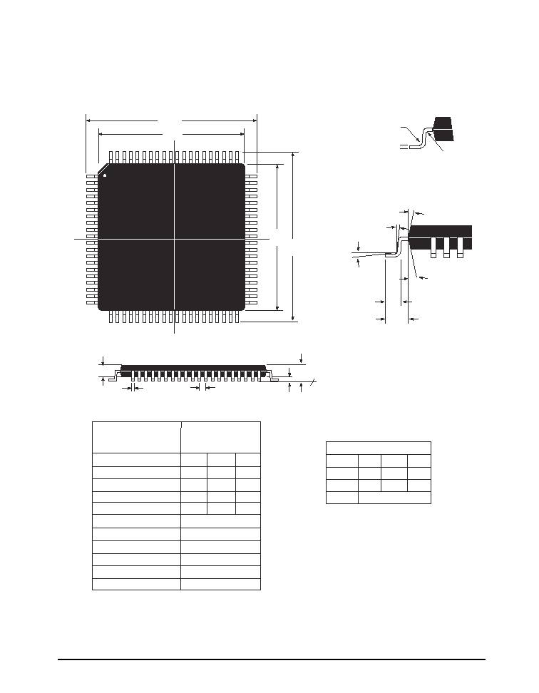
80 PIN LQFP
CL
b
e
L
11
∞
- 13
∞
0
∞
Min
11
∞
- 13
∞
0
∞
≠7
∞
0.2 RAD MAX.
0.08 RAD MIN.
DIMENSIONS
Minimum/Maximum
(mm)
SYMBOL
A
A1
A2
b
D
D1
e
E
E1
N
80-PIN LQFP
JEDEC MS-026
(BEC) Variation
MIN
NOM
MAX
1.60
0.05
0.15
1.35
1.40
1.45
0.22
0.32
0.38
16.00 BSC
14.00 BSC
0.65 BSC
16.00 BSC
14.00 BSC
80
c
L1
A2
COMMON DIMENTIONS
SYMBL MIN
NOM
MAX
c
0.11
23.00
L
0.45
0.60
0.75
L1
1.00 BASIC
Seating
Plane
A1
A
A
PIN 1
E1
D1
D
CL
E
PACKAGE: 80 Pin LQFP
20
Rev. 3/05/04
SP514 Multi≠Mode Serial Transceiver
© Copyright 2004 Sipex Corporation
ORDERING INFORMATION
Model
Temperature Range
Package Types
SP514CF ........................................................................... 0
∞
C to +70
∞
C ....................................................... 80≠pin JEDEC (BE-2 Outline) LQFP
Sipex Corporation reserves the right to make changes to any products described herein. Sipex does not assume any liability arising out of the
application or use of any product or circuit described hereing; neither does it convey any license under its patent rights nor the rights of others.
Corporation
ANALOG EXCELLENCE
Sipex Corporation
Headquarters and
Sales Office
233 South Hillview Drive
Milpitas, CA 95035
TEL: (408) 934-8700
FAX: (408) 946-9001
Sales Office
22 Linnell Circle
Billerica, MA 01821
TEL: (978) 667-8700
FAX: (978) 670-9001
e-mail: sales@sipex.com
DATE
REVISION
DESCRIPTION
3/05/04
A
Implemented tracking revision.
REVISION HISTORY